博文
理性设计Nd3+1.06um的近红外长余辉材料
|||
Designing thermally stimulated 1.06 μm Nd3+emission for the second bio-imaging window demonstrated by energy transfer from Bi3+ in La-, Gd-, Y-, and LuPO4
文章链接:https://www.sciencedirect.com/science/article/pii/S1385894719309039
Abstract
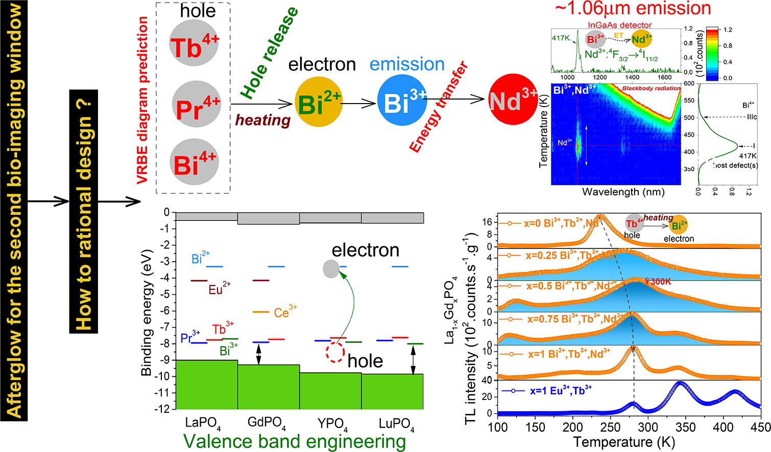
We report a general methodology to the rational design of thermally stimulated short-wave infrared (SWIR) luminescence between ~900 and 1700 nm by a new combination of using efficient energy transfer from Bi3+ to Nd3+ and an adjustable hole trap depth via valence band engineering. Predictions from a vacuum referred binding energy (VRBE) diagram are combined with the data from optical spectroscopy and thermoluminescence to show the design concept by using bismuth and lanthanide doped rare earth ortho-phosphates as model examples. Nd3+with its characteristic 4F3/2 → 4Ij (j = 9/2, 11/2, 13/2) emission in the SWIR range is first selected as the emitting centre. The energy transfer (ET) processes from Bi3+ or Tb3+recombination centres to Nd3+ are then discussed. Photoluminescence results show that the energy transfer efficiency of Bi3+ → Nd3+ appears to be much higher than of Tb3+ → Nd3+. To exploit this ET, thermally stimulated Bi3+ A-band emission can then be designed by using Bi3+ as a ~2.7 eV deep electron trap in YPO4. By combining Bi3+ with Tb3+, Pr3+, or Bi3+ itself, the holes trapped at Tb4+, Pr4+, or Bi4+ will release earlier than the electrons captured at Bi2+. On recombination with Bi2+, Bi3+ in its excited state is formed generating Bi3+ A-band emission. Due to the ET of Bi3+ → Nd3+ 1.06 μm Nd3+ emission appears in YPO4. Herein, the thermally stimulated Nd3+ SWIR emission is achieved by hole release rather than the more commonly reported electron release. The temperature when thermally stimulated Nd3+ SWIR emission appears can further be engineered by changing the Tb3+ or Pr3+ hole trap depth in Y1−xLuxPO4 by adjusting x. Such valence band engineering approach can also be applied to other compounds like La1−xGdxPO4 and Gd1−xLaxAlO3 solid solutions. Our work opens the avenue to motivate scientists to explore novel SWIR afterglow phosphors in a design way instead of by trial and error approach.
https://blog.sciencenet.cn/blog-497509-1191070.html
上一篇:Bi3+吸引电子与空穴的双重作用
下一篇:利用真空能级理性设计储能材料 (afterglow phosphor and storage phosphor)
全部作者的其他最新博文
- • 如何利用镧系和铋离子实现陷阱中电子与空穴运动的管理:同时实现X-ray成像,防伪与力的存储
- • Bi3+长余辉发光材料及其在防伪和X射线成像方面的应用
- • 设计LiTaO3:Ln3+,Eu3+ (Ln = Tb or Pr)光存储材料及其在防伪和柔性X射线成像应用
- • 吕天帅Laser & Photonics Reviews: 多功能和高性能LiTaO3:Tb3+, Gd3+
- • 吕天帅Chemical Engineering Journal: LiTaO3:Ln3+,Eu3+光存储材料
- • 吕天帅Materials Chemistry Frontiers: LiLuGeO4:Bi3+,Ln3+光存储材料